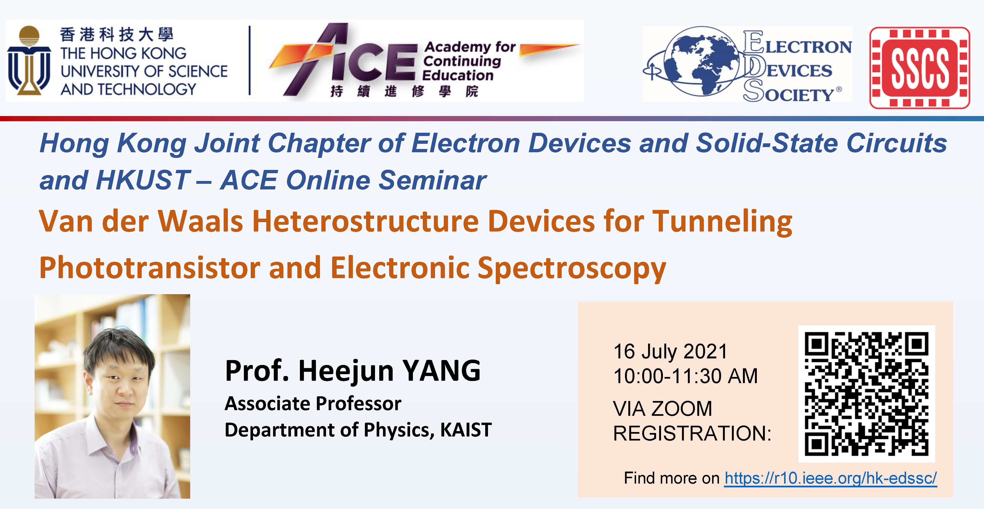
Each atomic layer in van der Waals heterostructures possesses a distinct electronic band structure that can be manipulated for unique device operations. In the precise device architecture, the subtle but critical band coupling between the atomic layers, varied by the momentum of electrons and external electric fields in device operation, has not yet been presented or applied to designing original devices with the full potential of van der Waals heterostructures. I will introduce interlayer coupling spectroscopy at the device-scale based on the negligible quantum capacitance of two-dimensional semiconductors in lattice-orientation-tuned, resonant tunneling transistors. The effective band structures of the mono-, bi-, and quadrilayer of MoS2 and WSe2, modulated by the orientation- and external electric field-dependent interlayer coupling in device operations, could be demonstrated by the new conceptual spectroscopy overcoming the limitations of the former optical, photoemission, and tunneling spectroscopy [1]. Based on the vertical heterojunction, novel orbital-gating based phototransistors and self-selective memristors [2,3] could be developed.
[1] Adv. Mater. (2020) [2] Nat. Commun. (2019) [3] Sci. Adv. (2021)
Biography
Heejun Yang was awarded the IUPAP Young Scientist Prize in Semiconductor Physics 2018 for his outstanding contribution to novel interface devices based on structural, electronic, and quantum-state control with van der Waals layered materials. He received his PhD in physics with a subject on graphene by scanning tunneling microscopy and spectroscopy (STM/STS) from Seoul National University (Korea) and University Paris-Sud XI (France, a joint degree) in 2010, and experienced industrial device studies in Samsung Electronics from 2010 to 2012. Then, he conducted his research on graphene spintronics in Albert Fert’s (2007 Novel laureate) group in CNRS/Thales as a postdoc from 2012 to 2014. With his research background on molecular and nanometer-scale studies (in Seoul and Paris) and electric and spintronic device physics (in Samsung and CNRS/Thales), he moved to Sungkyunkwan University (2014~2021) and KAIST (2021~) and started original device studies with phase engineering of low-dimensional materials.

